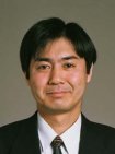
Rossella Brunetti / University of Modena

Upcoming Physics Challenges for Device Modeling
When something (material, device, system or process) is developed on a truly nanometric scale its behavior becomes different from the one observed on the submicron mesoscale. Nanoscience and nanotechnology offer challenging problems to fundamental research and new opportunities for innovative industrial applications. Furthermore, an impressive merging of knowledge is taking place with the molecular-biology community. The progression from “micro” to “nano” of the semiconductor science and technology seems to be a natural evolution imposed by the miniaturization requirements. However “from the lab to the market” is a long way for anything build on the nano scale. At present there are many good ideas, some engineered prototypes, but only few industrial applications. This talk will provide an overview on some innovative ideas for nano devices and sensors and illustrate to which extent they can, at present, realistically compete with the performances offered by the conventional products of the semiconductor industry. Examples of nano components for quantum computation, bioinspired sensors, molecular devices, and non-volatile nano memories will be given.
Rossella Brunetti received the Laurea cum laude in Physics in 1981 and the Ph. D. in Physics at the University of Modena in 1987. She has been working at the Physics Department of the University of Modena as research assistant since 1990 and as teaching and research assistant from 1993. From 2002 Rossella Brunetti is an associate professor in Physics at the Physics Department and the Pharmacy Faculty of the University of Modena and Reggio Emilia. The research activity carried on after the laurea until now has been concerned with electron transport in semiclassical and quantum conditions in semiconductor structures and devices. Rossella Brunetti has experience with a variety of numerical techniques (mainly the Monte Carlo approach and, more recently, Molecular Dynamics) which have been applied to obtain results for many different semiconductor systems. During the last ten years most of her scientific activity has been devoted to quantum transport problems in mesoscopic structures and low-dimensional systems. In particular, she recently studied electronic coherent transport properties in systems of coupled quantum wires in view of possible applications to quantum computation devices. In the last years Rossella Brunetti created a research team aimed at the formulation of a simulative model based on coupled Molecular Dynamics and Monte Carlo techniques for the analysis of single-channel ion current and noise. The research activity has been focused on the case of potassium ions permeating the KcsA channel, but the method can be extended to the analysis of other channels, provided that the atomic structure of the channel protein is available from diffrattometric analyses.
Toshiro Hiramoto / University of Tokyo

Transport in Silicon Nanowire and Single-Electron Transistors
Toshiro Hiramoto received B.S., M.S., and Ph.D degrees in electronic engineering from the University of Tokyo in 1984, 1986, and 1989, respectively. In 1989, he joined Device Development Center, Hitachi Ltd., Ome, Japan, where he was engaged in the device and circuit design of ultra-fast BiCMOS SRAMs. In 1994, he joined Institute of Industrial Science, University of Tokyo, Japan, as an Associate Professor. He was also an Associate Professor in VLSI Design and Education Center, University of Tokyo, from 1996 to 2002. He is currently a Professor in Institute of Industrial Science, University of Tokyo. His research interests include low power and low voltage design of advanced CMOS devices, SOI MOSFETs, device/circuit cooperation scheme for low power VLSI, quantum effects in nano-scale MOSFETs, and silicon single electron transistors.
Dr. Hiramoto is a member of IEEE, IEICE, and Japan Society of Applied Physics. He has been an Elected AdCom Member of IEEE Electron Devices Society since 2001. He served as the General Chair of Silicon Nanoelectronics Workshop in 2003, and the Program Chair in 1997, 1999, and 2001. He also served on Program Subcommittee on Integrated Circuits of IEEE International Electron Devices Meeting (IEDM) in 1993 and 1994 and on Program Subcommittee on CMOS Devices of IEDM in 2003 and 2004, and has served on Program Committee of Symposium on VLSI Technology since 2001. He was the Subcommittee Chair of CMOS Devices of IEDM in 2005. He is the Asian Arrangement Co-Chair of IEDM in 2006 and 2007.
Chenming Calvin Hu / University of Berkeley
Compact Modeling for New Transistor Structures
Using embedded SRAM as a path, FinFET may enter manufacturing at 32nm. FinFET provides several advantages over the planar MOSFET structure----smaller size, larger current, smaller leakage, and less variation in threshold voltage. A compact model of multi-gate transistors will facilitate adoption of new-structure transistors. BSIM-MG is a surface-potential based compact model of multi-gate MOSFETs fabricated on either SOI or bulk substrates. The effects of body doping are modeled. It can also model a double-gate transistor with independently biased front and back gates and asymmetric front and back gate work-functions and dielectric thicknesses.
Chenming Calvin Hu is the TSMC Distinguished Chair Professor of Microelectronics in Electrical Engineering and Computer Sciences at University of California, Berkeley. He was the Chief Technology Officer of TSMC, world's largest dedicated integrated circuits manufacturing company from 2001 to 2004. He was the founding chairman of Celestry Design Technologies that was acquired by Cadence Design Systems in 2002. He was the board chairman of the non-profit East Bay Chinese School, Oakland, CA. He is the author or co-author of three books and 800 research papers and has supervised 60 doctoral students in the field of semiconductor technology. Dr. Hu is a member of the US National Academy of Engineering and Academia Sinica; a fellow of the IEEE and the Institute of Physics and an Honorary Professor of the Chinese Academy of Science Microelectronics Institute, and National Chiao Tung University. In 1997, Dr. Hu received the IEEE Jack A. Morton Award for contributions to transistor reliability physics. In 1999, he received the DARPA Most Significant Technological Accomplishment Award for co-developing FinFET. In 2002, he received the IEEE Solid State Circuits Award for the BSIM transistor model. He has also received UC Berkeley's highest honor for teaching - the Berkeley Distinguished Teaching Award. Dr. Hu received his B.S. degree from National Taiwan University and M.S. and Ph.D. degrees from University of California, Berkeley, all in electrical engineering. He enjoys painting with his sons, Raymond and Jason.
Peter Pichler / Fraunhofer Institute

Upcoming Challenges for Process Modeling
In industrial environments, numerical simulation has become an indispensable tool for the development and optimization of especially front-end processes. In order to remain useful for future technology nodes, process simulation has to follow and partly even anticipate paradigm shifts of state-of-the-art processes and new materials for future nanoelectronic devices. Within this talk, the author presents his personal view of unsolved and upcoming issues that have to be addressed and solved in future.
Peter Pichler obtained the Dipl.-Ing. degree in Electrical Engineering in 1982 and the Dr. techn. degree 1985 both from the Technical University of Vienna. Since 1986 he is Group Manager at Fraunhofer IISB, responsible for diffusion modeling and simulation activities. In 2004 he got the venia legendis from the University of Erlangen-Nuremberg. Dr. Pichler contributed to various European projects, coordinated the ESPRIT LTR projects RAPID and the IST project FRENDTECH, and coordinates the IST project ATOMICS. He is the author or coauthor of more than 70 publications in international journals and conference proceedings, and author of the book “Intrinsic Point Defects, Impurities, and Their Diffusion in Silicon” published by Springer Wien-New York.
Mark Pinto / Applied Materials, Inc.

Nanomanufacturing Technology and Opportunities Through Physically-Based Simulation
Mark R. Pinto is the chief technology officer, senior vice president and general manager of the New Business and New Products Group at Applied Materials. Appointed to this role in January 2004, Dr. Pinto is responsible for Applied's technology direction, its advanced R&D programs and for developing new business opportunities. His group includes several high-growth businesses, including equipment and services for the flat panel display industry, as well as, the company's 2006 entry into the solar photovoltaic equipment market. He also is responsible for Applied's IP licensing business and serves as Chairman of Applied's Venture Investment Committee.
Previously, Dr. Pinto spent 19 years with Bell Laboratories and the Lucent Microelectronics Group, later to become Agere Systems. His most recent assignments had been as vice president and general manager of a network product IC division and as chief technology officer where he led all central IC and optoelectronics R&D. He was named a Bell Labs Fellow, the company's highest technical honor, for his contributions to semiconductor devices and simulation.
Dr. Pinto received bachelor's degrees from Rensselear Polytechnic Institute and a master's degree and Ph.D. from Stanford University. As part of his doctoral work, he developed the device simulator PISCES-II, which was a standard tool in the industry for many years. Dr. Pinto has authored or co-authored more than 150 papers and has nine patents. He has been active in industry consortia including serving on the board of directors of Semiconductor Research Corporation and the Technology Strategy Committee of the Semiconductor Industry Association. He is also a Fellow of the IEEE and served as an Adjunct Professor at Yale University.
